
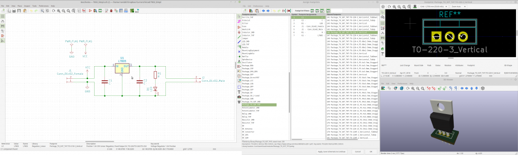
KiCAD abstracts the Symbols on a Schematic from the Components on the PCB. To get from one to the other we need to assign a Footprint to each Symbol. There are multiple ways to accomplish this, we will start with the batch tool to do all of them at once for the Basic 7805.
Basics:
The Footprint describes the physical appearance of the Symbol for position on the PCB. It gives the PCB the means to place the Component represented by the Schematic Symbol.
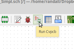
Prior to adding Components to the PCB footprints need to be assigned to all the Schematic Symbols. Clicking the “Run Cvpcb” icon. ( this is the tool that assigns the footprint ) The”Assign Footprints” window will be presented
Footprint Assignment – Batch
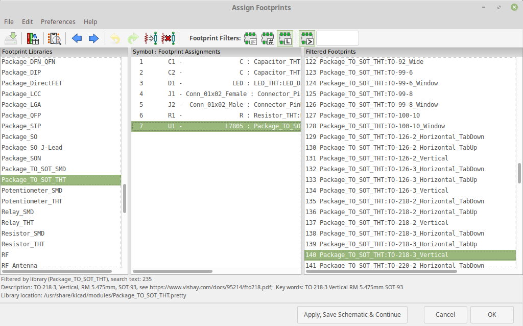
The tool has three columns in its main windows
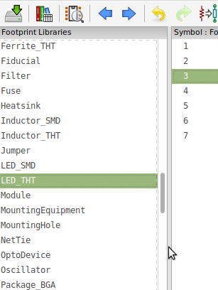
“Foot Print Libraries”
The Leftmost column contains a categorized list of available footprints. Selecting an Item in this column will filter the items in”Filtered Footprints”
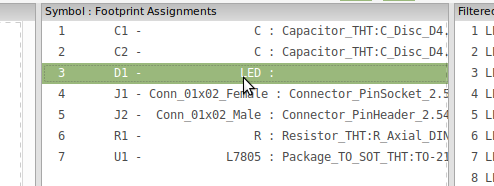
Symbol: Footprint Assignments
The middle column contains a list of the Symbols in your Schematic and the Footprint currently assigned.
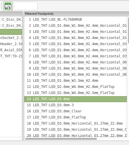
Filtered Footprints.
The right most column contains a list of footprints to assign.
This is a process to assign a footprint.
- Select the Symbol from the middle colum
- Select the correspond library from the left hand cloum
- Double-Click the item in the left hand colum you wish to assign.
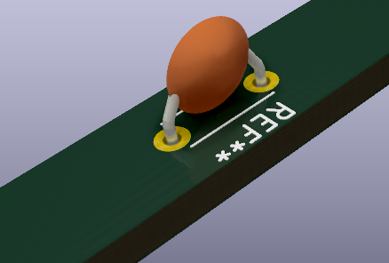
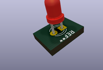
Let’s try it with the LED
From the Schematic Editor AKA Eeschema Click the “Assign Footprints” Icon
When the “Assign Footprints” window appears , click the LED in the middle colum
In the left hand column click the Footprint Library , LED_THT ( THT Stands for through hole )
For our lesson we will pick the Footprint “LED_THT:LED_D3.0mm”. ( You can customize for different sized LEDs fairly easily) Double click this entry
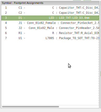
The “Symbol: Footprint Assignments” should now reflect your choice.
Within each Footprint there are “Hidden Descriptors” Things like Diameter will be D followed by a number, Pitch is P followed by a number.
Here are the categories for each Symbol
- Capacitor_THT
- LED_THT
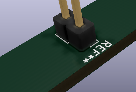
- Connector_PinSocket_2.54
- Connector_PinHeader_2.54mm
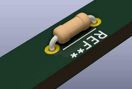
- Resistor_THT
And the Footrints I chose in each case
- Capacitor_THT:C_Disc_D4.3mm_W1.9mm_P5.00mm
- LED_THT_LED_3.0mm
- Connector_PinSocket_2.54mm:PinSocket_1x02_P2.54_Vertical
- Connector_PinHeader_2.54mm:PinHeader_1x02_P2.54_Vertical
- Resistor_THT:R_Axial_DIN0204_L3.6mm_D1.6mm_P5.08mm_Horizontal
Using the method above add all the footprints.
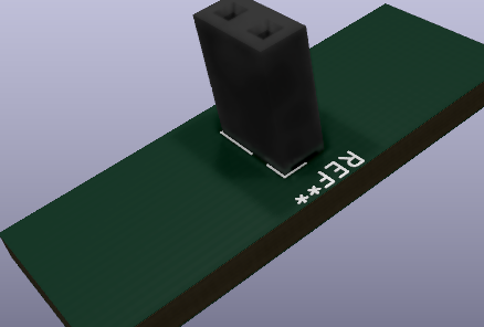
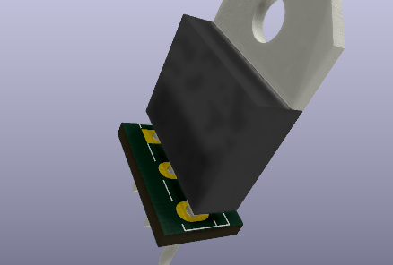
Lastly the Transistor
Let’s Walk through the process with the Transistor as it is slightly more complicated.
Click U1 in the Middle Window
Select Package_TO_SOT_THT in the library window.
NOTE: Various Transistors and ICs come in a variety of Form Factors. The electrical characteristics may be the same or similar, the Footprint is describing the physical attachment and sizes.
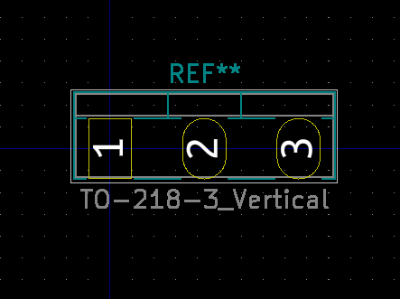
In my case I am using a 3-Pronged, Vertical , Through Hole, with a heatsink atachment.
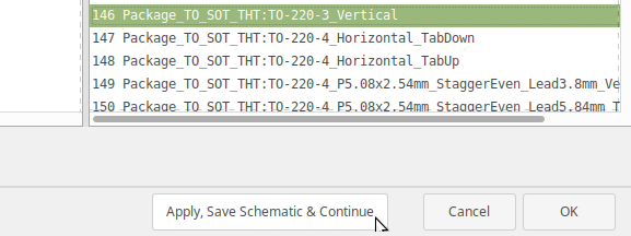
Select Package_TO_SOT_THT:TO-220-3_Vertical
When you feel you have assigned all the items correctly. Click on the “Apply, Save Schematic & Continue”, then click Ok.
That is it for Footprint Assignment, Next up is laying out the PCB