
After we have created a Schematic, Annotated and assigned Footprints we can create a PCB and bring in components from the schematic.
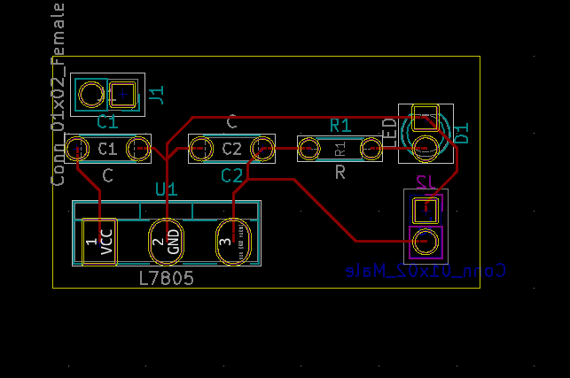
Come Back Soon! This is in progress. Should be done by Friday July 10th. If you just can’t wait you might be able to muddle through with the diagram below. I still need to hookup J1 tho.
Get the Symbols from Schematic
The first thing we will need to do is “import” the components, using the symbols from the schematic. This process will use the Footprints we assigned previously to place the Components base on the Symbols we selected in the Schematic. ( You might want to read that a few times.)
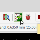
Find the “Push Changes tool in the toolbar at the top of the screen, it is a PCB with a Green arrow. You can also use the “Update PCB from SChematic” in the Tools Menu.
When you get teh “Update PCM from Schematic” Window simply click “Update PCB”
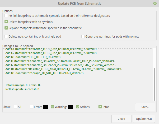
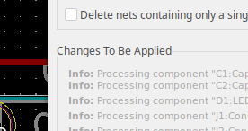
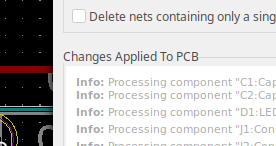
If you see the green message “Netlist update successful!”,
Click Update to Apply the Changes, the message window will change from “Changes to Be Applied” to “Changes Applied To PCB”
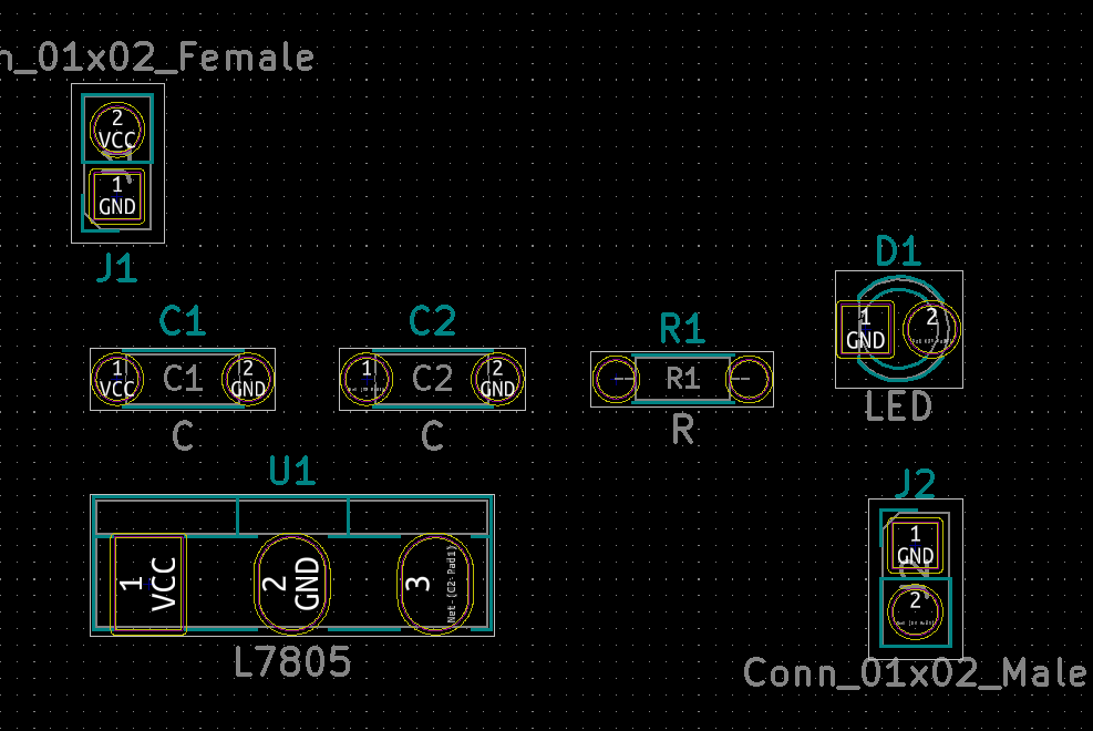
Now close the window and you should see a clump of components attached to your cursor. Click somewhere in the middle of the layout drawing ( it doesn’t matter exactly where ).
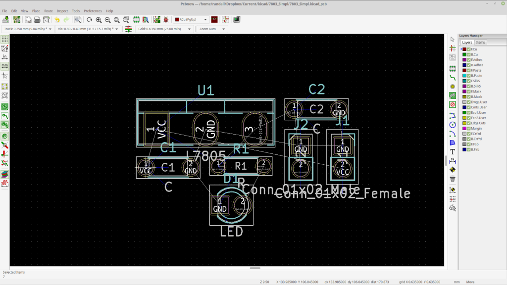
Positioning the Components
Select
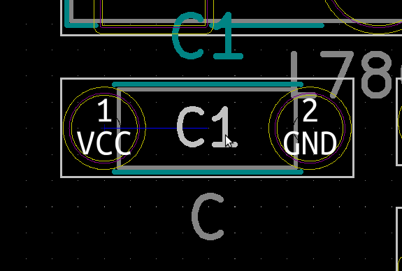
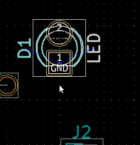
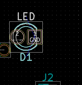
To drag a component into position first click the component, making sure you have the whole thing selected. Often you will select just a label instead of the whole group. Compare the two figures below, notice how all the parts are highlighted in the second figure, whereas in the first only the labels.
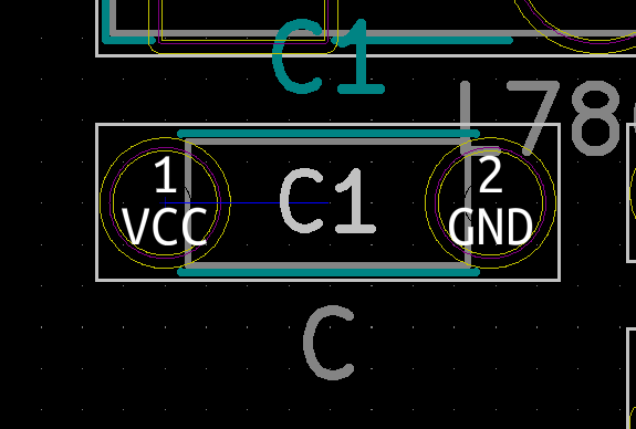
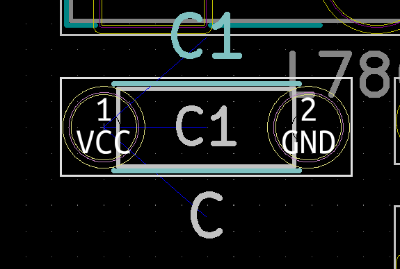
This can be frustrating so let’s look a little more. Click within the bounds of the component but not on/near labeling will select the whole component. Clicking on the lettering will select the lettering. Notice the mouse position in the following two figures.

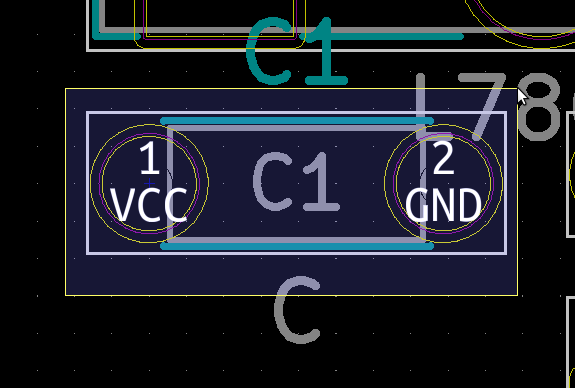
Finally we can use box select if the mouse select is not working. You can click in an empty area and drag to use box select.
Move
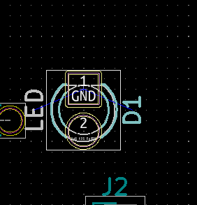
When you have the component selected drag it near its final position, by pressing M ( for “Move” ) Position them as shown in the following figure.
NOTE: You can also access move in the context menu by right clicking on the selected item.
Rotate
When the items are positioned we will rotate some of them. Let’s learn how with the LED>
Select the LED
Press “R” three times so that GND is at the Top.
Re-position the LED so it is back where it started before rotation
We could have also used Shift-R, to rotate counter-clockwise and only have to press the keys once.
Repeat this procedure for J1, so the GND sits on the right.
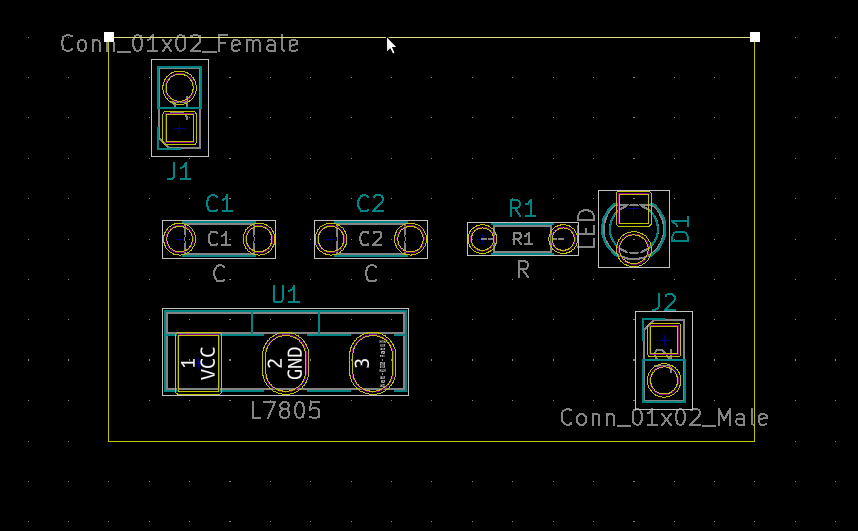
Adding an Edge
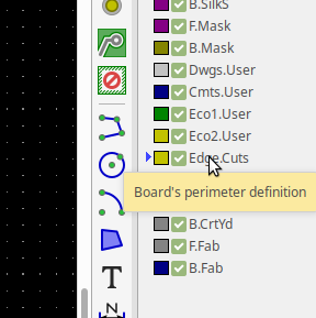
We will need to tell KiCAD where the edges of the PCB will be, this is how the Manufacturer will cut the PCB.
Select Edge Cuts the Layer
Set the Grid Snap to 2.54 ( Just helps to make straight lines and corners )
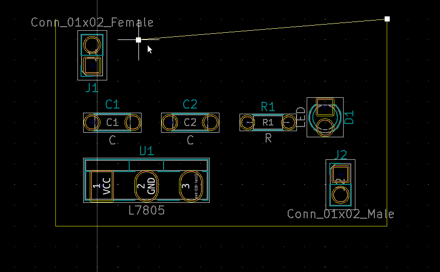
Use the Line tool, Draw four lines around the components
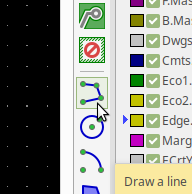
Click Line Tool, CLick Start Point, Click Stop Point
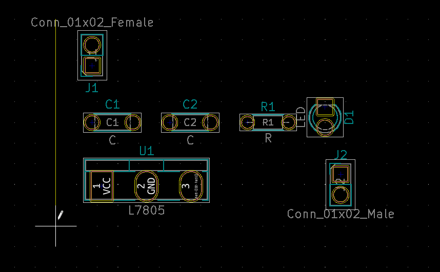
The line tool will continue, form the endpoint of the first line so you can just work your way around to create the rectangle.
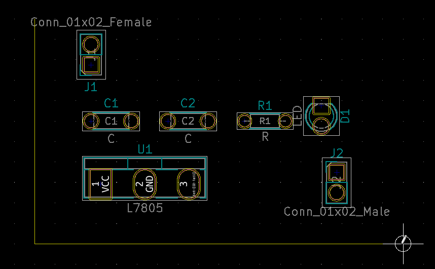
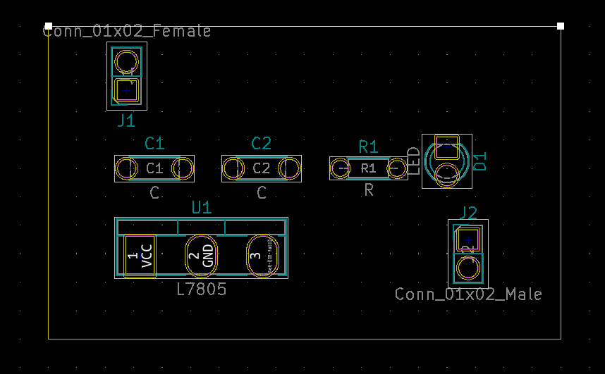
If aline is misplaced click the line to select, click and hold the small white square to reposition.
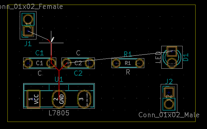
Wiring the Components
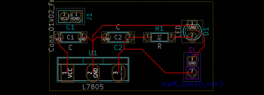
Using the wiring tool, let’s add tracks for each of the Components.
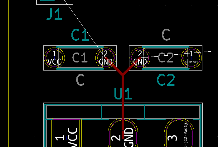
We will start by laying tracks for GND
Click the “Push Pull Router” tool on the right side of the screen OR press X
NOTE: This is the same as the menu item Route->Route a single Track
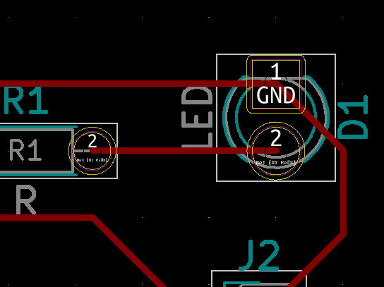
On U! click the middle pad numbered 2 and labeled GND.
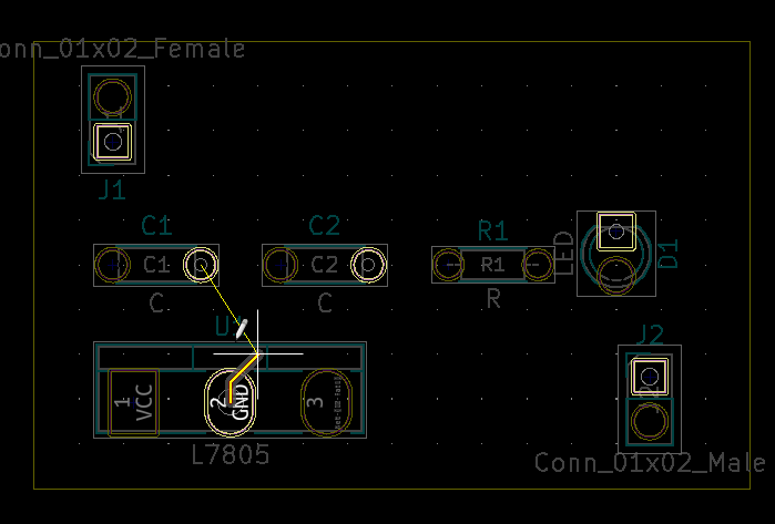
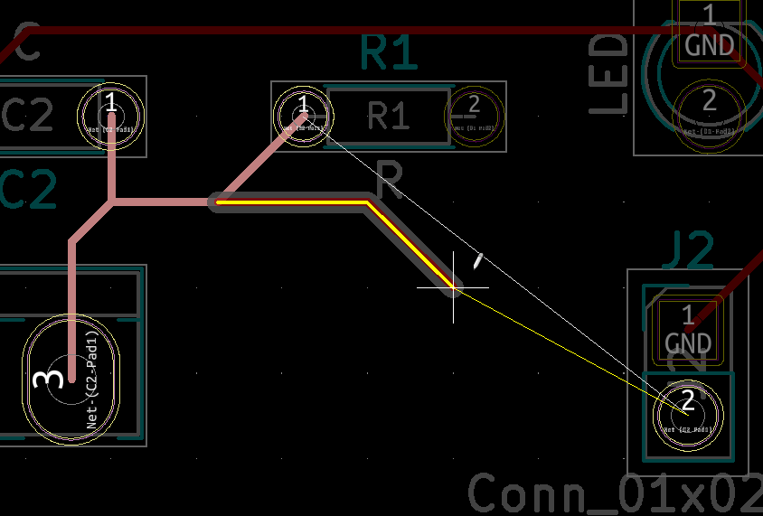
Candidates for wiring will be highlighted. This information comes from your schematic. You will see a thick yellow line that denotes where your track will lay down. A second thin yellow line shows the nearest item in that “net”.
Click the C1 Capacitor above and slightly to the left, a track will be laid down.
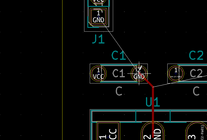
Rotate and Reposition C2 using what you learned previously and wire GND the same way. You can exit the Single Track tool by pressing escape or click the selection arrow. Try to get your track similar to below.
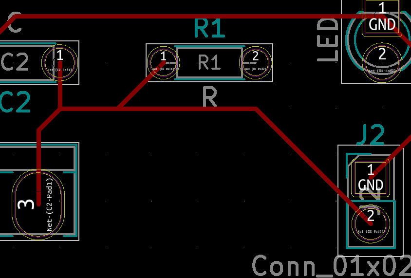
To add an extra bendpoint in the track click once where you would like the bendpoint to be positioned .Finish up the GND Net as follows:
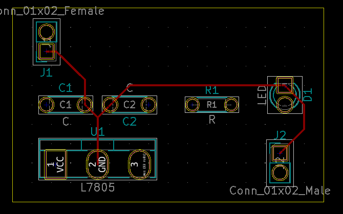
Connect the remaining GND net
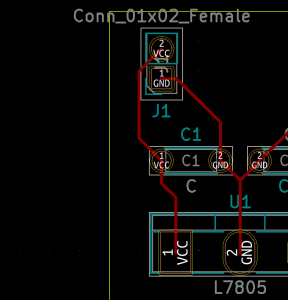
Wire the VCC network on the left side by connecting J1 VCC, C1 VCC and U1 VCC, If you cant see the VCC designation you can zoom in with your mouse wheel.
Wire the VCC network on the left side by connecting J1 VCC, C1 VCC and U1 VCC, If you cant see the VCC designation you can zoom in with your mouse wheel.
Wire the output ( +5v ) from U1 to the resistor, and J2. When running tracks you can select an existing track as a starting point for the next track
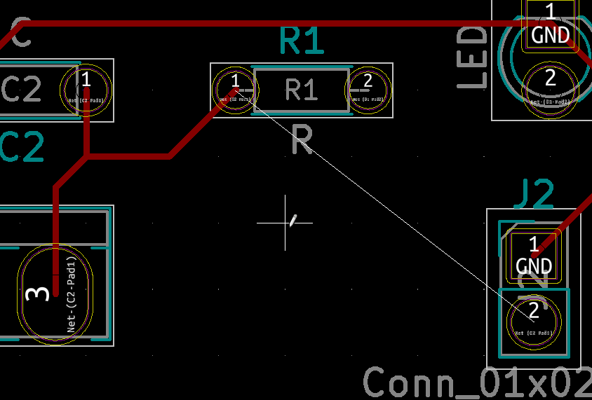
Lastly, wire the R1 Resistor to the number 2 pad on the LED
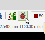
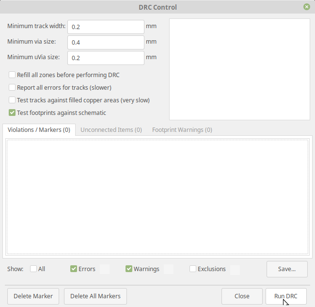
As final check run the DRC. This is a built in Design Rules Checker. It helps to highlight conman mistakes and problems with your board. Rules here can be broken but this is a great starting point. I will help you find items that may look connected but are note. Launch the DRC by clicking the bug.
Run the DRC by clicking the “Run DRC”. If all is well you will be ok to go to the Manufacturer. If not take a look at the article on troubleshooting your PCB ( not completed yet ).
The next upcoming article will be on Manufacturing your PCB , sending it out.